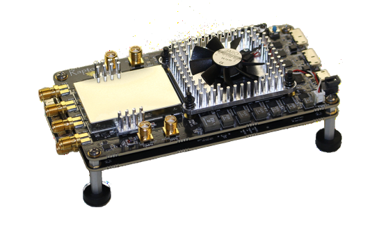
SDR System is a complex RF development platform intended to operate over a frequency range of 70 MHz to 6000 MHz with a tunable channel bandwidth from 200 KHz to 56 MHz. The receiver shall receive signals in the aforesaid frequency and down converts it to an IF frequency. This down converted IF signal shall be processed by users’ customized signal processing algorithms. The baseband processing module shall be of Zynq based FPGA and there shall be a provision to port user specific application programs along with demodulation schemes. The user developed Embedded modules shall be ported on to the integrated ARM processor and the same shall be sent out to a host system through 1GbE LAN interface. There shall also be provision to support ethernet based RF configurations for the RF platform.
The transmitter module should use a direct conversion architecture that should achieve high modulation accuracy with ultralow noise figures. The transmitted design should allow significant system margin for the external power amplifier (PA) section. The on board Transmit power monitor should have provision such that it operates at highly accurate Tx power and does the power measurements.
The system shall consist of the following Functions/Modules:
- RF Transceiver Module
- Zynq FPGA based Baseband Processing Module
- Audio Interface Module
- 1GbE Control Interface Module
- Mechanical Enclosure
- Power Supply Module
Technical Specifications:
| S.No | Parameters/Features | Specifications/Value |
| 1) | Receive Chain Module : It should support the following features | |
| 1.1 | Frequency Range | Configurable 70 to 6000 MHz |
| 1.2 | Tunable channel bandwidth | 200 kHz to 56 MHz |
| 1.3 | Noise Figure | < 4dB |
| 1.4 | Gain | 0 to 60 dB |
| 1.5 | Receiver gain control | 0-60 dB in steps of 1 dB |
| 1.6 | Second-Order Input Inter modulation Intercept Point | 40 – 45dBm |
| 1.7 | RF input channels | 2 |
| 1.8 | Tuning Resolution | 2.4Hz |
| 1.9 | LO Leakage | -90 to -125 dBm |
| 1.10 | Channel Isolation | <70 dB |
| 2) | Transmit Chain Module : It should support the following features | |
| 2.1 | Frequency Range | Configurable 70 to 6000 MHz |
| 2.2 | Power Gain Control | 0 to 60 dB |
| 2.3 | TX Gain control | 0-60 dB in steps of 1 dB |
| 2.4 | Second-Order Input Inter modulation Intercept Point | <25 dBm |
| 2.5 | RF Output channels | 2 |
| 2.6 | Channel Isolation | <50 dB |
| 2.7 | Transmit power | 0 dBm |
| 3) | LO Synthesizer Module: It should support the following features | |
| 3.1 | LO Frequency Step | 2.4 Hz |
| 3.2 | Reference Clock | 10-80 Mhz |
| 3.3 | Clock signal level | 1.3vp-p |
| 4.0 | Base Band Processing Module: It should support the following features | |
| 4.1 | Analog Converter Module ADC with Resolution DAC with Resolution | 12 bits 10 bits |
| 4.2 | FPGA : It should support the following features | |
| FPGA | Zynq FPGA SoC, XCZ7035 | |
| Non-Volatile Memory | 4GB SDMMC/ eMMC | |
| SDRAM | DDR3L, 1GB | |
| Program and debug interfaces | JTAG | |
| Serial interfaces | UART, SPI | |
| Ethernet | 1 Gbps | |
| ADC, DAC interface/Transceiver Interface | LVDS | |
| 4.3 | FPGA Firmware Module: It should support the following features | |
|
RF Data interfaces logic should be implemented in FPGA API drivers should be
provided FPGA project should be provided to us to implement our algorithms |
||
| 4.4 | Peripheral audio input interface | |
| 6.0 | Other Details | |
| 6.1 | Operating temperature | 0 to +50 C |
| 6.2 | Power Input | 230 AC /12V DC |
